About Us
Combining the Best of Semiconductor Industry,
Nanoscience and Biotechnology
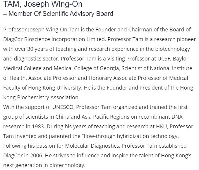
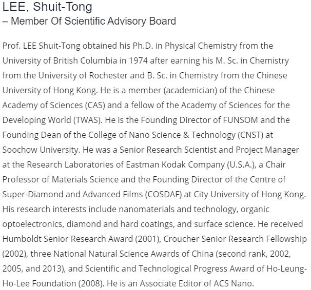
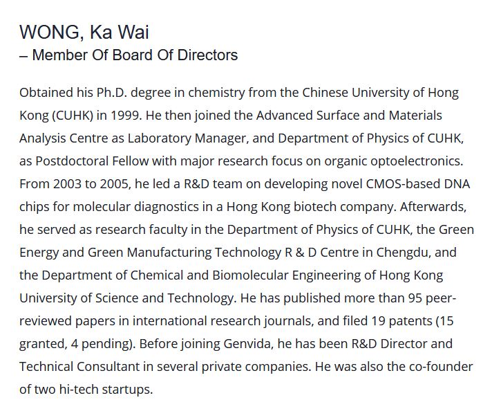
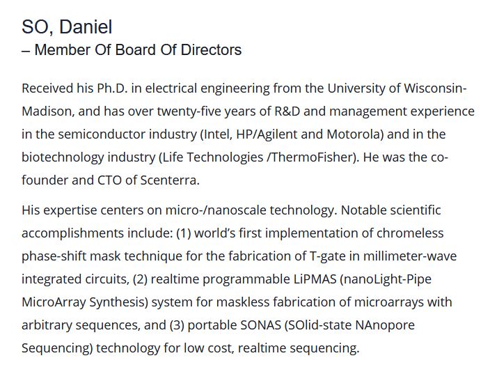
With the foresight to see the marriage of hi-tech with biotech to solve biological problems in a much more cost effective and time saving manner, Genvida was founded by the experts from the IC and nano-scale industries, and leaders in the high-throughput genomics sciences.
Genvida’s technologies and innovations are the fruits of the founding team-members’ 100+ years of combined working experience in science and engineering, and are covered by Genvida’s granted / pending patents in China, the European Union, Japan, Korea and the United States. The covered areas include sample preparation, micro-/nanofluidics architecture, solid-state nanopore fabrication, detector design, sequencing methods, system design, and bioinformatics. With this wide-ranging coverage, Genvida has created an environment that competitors cannot easily penetrate.
Milestones
-
- Applied the 1st US Patent for nanodevices technologies
- Explored the in-situ nanopores etching method directly on silicon wafer
- Initiated the idea for using nanochip in bioinformatics
-
- Genvida was founded with the support of seeding Fund
- Received the 1st batch of international patents for speeding-up the development of SONAS® platform
-
- Completed Series A angel investment
- Received funding from the venture capital under Innovation and Technology Commission of HKSAR
- Setup headquarter and laboratory in Hong Kong Science and Technology Parks
- Designed and completed the installation of proprietary nanopore vacuum etching system
- Completed the installation of picoampere monitoring system for nanochip
- Signed strategic partnership agreement with research institutions in New York, Beijing and Hong Kong
-
- Etched 50nm diameter nanopores on chip in our proprietary system
- Completed the trademark registration of “SONAS” sequencing platform in USA and China
-
- Achieved 10.8nm nanopores in the first half of the year
- Nanopores size further reduced to 5nm in September
- Received US patent of nano devcies using for DNA sequencing
- Signed co-development agreement with reputable semiconductor company in Europe for wafer supply


